Process for fabricating a field-effect transistor device implemented on a network of vertical nanowires, the resulting transistor device, an electronic device comprising such transistor devices and a processor comprising at least one such device
Référence
03903-01
Mots-clés
Statut des brevets
FR Priority patent application FR1059802 filed on 11/26/2010 and entitled “Procédé de fabrication d’un dispositif de transistor à effet de champ implémenté sur un réseau de nanofils verticaux, dispositif de transistor résultant, dispositif de transistors, et processeur comprenant au moins un tel dispositif électronique »
US patent 13/989509 filed on 11/24/2011.
EP patent 2643848 published on 10/02/2013.
Jp patent 2013-540371filed on 11/24/2011.
Kr patent 10-2013-7013576 filed on 11/24/2011
Inventeurs
Guilhem LARRIEU
Statut commercial
Exclusive or non-exclusive license
Laboratoire
Description
CONTEXT
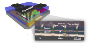
The present invention relates to a process for fabricating a field-effect transistor device implemented on a network of vertical nanowires, including a plurality of elementary transistors.
TECHNICAL DESCRIPTION
Each elementary transistor comprising a source electrode and a drain electrode each positioned at one end of a vertical nanowire of the network and connected by a channel and each elementary transistor including a gate electrode surrounding each vertical nanowire of the network, the drain, source and gate electrodes of the elementary transistors implemented on the nanowires are respectively connected to each other so as to form unique drain ,source and gate electrodes of the transistor device
DEVELOPMENT STAGE
This process has been successfully implemented on a matrix of 650 nanowires with gate length of 15nM and with electricals results at the state of the art.
BENEFITS
The invention therefore aims to significantly simplify the fabrication of the transistor devices implemented on a network of vertical nanowires, to be able to decrease their dimensions to nanoscale regimes and to minimize the access resistances of the source and drain areas as well as the overlap capacitances. The invention therefore aims to propose transistors having a low access resistance as well as low overlap capacitances.
INDUSTRIAL APPLICATIONS
These elementary transistor devices (nFET and pFET) can for example be used to produce logic circuits, such as CMOS inverters. According to other alternatives, these electronic devices belong to the group consisting of a CMOS inverter, a multiplexer, a volatile memory, a non-volatile memory, a device for detecting gases or biochemical agents. A processor according to the invention includes at least one electronic device as previously described.