Photo-crosslinkable emissive molecular materials
Référence
07293-01
Statut des brevets
French priority patent application filed on February 23rd, 2015 and entitled “MATÉRIAUX MOLÉCULAIRES ÉMISSIFS PHOTOPOLYMÉRISABLES”
Pending Patent applications in: Europe; Korea; United States of America; Japan
Inventeurs
Olivier SIMON; Bernard GEFFROY; Elena ISHOW; Tony MAINDRON
Statut commercial
Exclusive or non-exclusive license
Laboratoire
Laboratoire CEISAM – Chimie Et Interdisciplinarité: Synthèse, Analyse, Modélisation
http://www.sciences.univ-nantes.fr/CEISAM/
UMR 6230, Nantes, France
Description
Context
OLED fabrication requires multilayered structures that have mostly been obtained upon vacuum evaporation. Such process is not suitable for large-area devices at low costs and faces molecular reorientations leading to large performance loss. The current invention overcomes these limitations by offering an all-solution deposition process, yielding multi-stacked architectures of charge-transporting and light-emitting layers using photo-crosslinkable small fluorescent molecules. Successive cycles of wet deposition and photoirradiation can easily be performed to make the layer of interest insoluble with no risk of dissolving the previous ones. In this way, pixelized multicolor emissive structures can readily be achieved.
Technical description
The patent covers the synthesis of a family of small emissive molecules with high brightness in the solid-state, and amenable to form insoluble thin films of a high optical quality. These molecules comprise bulky and twisted structures to promote stable amorphous materials with no risk of crystallization, and photo-polymerizable acrylate- or oxetane-based units for photo-crosslinking at room temperature. Emissive layers are formed by spin-coating or ink-jet deposition and provide insoluble emissive patterns upon photoirradiation through the use odd masks at room temperature.
Development stage
OLEDs have been fabricated at the laboratory scale using a spin-coating or inkjet deposition process. Such process is compatible with any nature (plastics compatible with the employed solvent, glass) or geometry (flat, curved) of substrates and yields nanometer-thin films, structurally stable over years with no microcrystallite formation. .
Photo-crosslinked fluorescent organic nanoparticles serving as potential optical labels for bioimaging have been fabricated out of the series of molecules and photoirradiation process reported in the patent, and by resorting to microfluidic systems.
Benefits
This system combines a multifold of advantages:
- straightforward transferability of properties from solution to the solid-state;
- reproducibility of properties from batch to batch owing to the molecular structure of the emissive molecules;
- thin films with very smooth surface and high optical quality (RMS roughness less than 1.3 nm) due to the absence of segregation or crystallization;
- reduced costs of fabrication and loss of unused products;
- access to large electroluminescent panels, pixelized emissive surfaces, and 3D-fluorescent patterns.
Industrial applications
- OLED displays
- OLED lighting (multilayered OLED)
- Counterfeit detection using infrared emitting layers
- Fluorescent nanoparticles for bioimaging
- Holography
- Cosmetics
- Packaging
- Fine chemistry
- Smart textiles
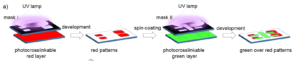
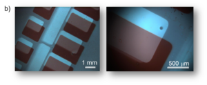
a) Schematic description for the fabrication of dual-color patterns from stacked photocrosslinked small fluorophores. B) Green and red emitting patterns using successive deposition and photoirradiation in the solid state of red and green small emitters endowed with photopolymerizable units (RMS roughness ~1.3 nm).