Process and device for fast atom diffraction in surface analysis
Référence
00021-01
Mots-clés
Statut des brevets
French patent application FR0606211 filed on July 7th, 2006 entitled: « Dispositif et procédé de caractérisation de surfaces »


Inventeurs
Philippe RONCIN
Hocine KHEMLICHE
Patrick ROUSSEAU
Statut commercial
Research agreement or exclusive licenses
Laboratoire
Laboratory Laboratoire des collisions atomiques et moléculaires, Université Paris Sud, (UMR 8625), a CNRS laboratory, Orsay, France, http://www.lcam.u-psud.fr/
Description
TECHNICAL DESCRIPTION
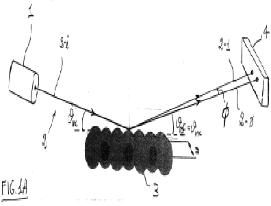
This invention describes a device and a process based on fast (100 to 1000 eV) atom diffraction for surface analysis. It makes it possible to determine the crystallographic structure of crystalline surfaces and control in real time crystal growth by molecular beams epitaxy.
The device is composed of an ion source (Fig1A-1), a neutralizer and a detection system (Fig1A-4). The beam of neutrals (Fig1A-2) is collimated and directed under grazing incidence (from 0.5° to 3°) on the sample surface (Fig 1A-3). The detection system consists of microchannel plates coupled to a phosphor screen, its high efficiency makes it possible to work with extremely low beam intensities, as compared to other techniques (RHEED).
![]() BENEFITS
BENEFITS
Because this technique uses atoms at grazing angles, it is sensitive only to the top surface layer and allows the study of insulating samples in a totally non destructive manner. This represents a major advantage compared to RHEED, which induces a charging of the surface and generally creates irreversible damage on this type of material.
INDUSTRIAL APPLICATIONS
This device finds its use in real time control of thin film growth and the study of crystallographic structures of semi-conductors and insulators. This device is fully compatible with Molecular Beam Epitaxy (MBE) systems.
Besoin de plus d'informations ?
Nous contacterTechnologies Liées
-
16.12.2014
Method for determining the chemical composition of a powder
Dispositifs & Instruments 05296-01
-
15.12.2014
Method for determining the particle-size distribution function in a powder
Dispositifs & Instruments 01880-02
-
15.12.2014
Method for determining the radius and/or particle density of a powder
Dispositifs & Instruments 01880-01