Method for producing a monolithic electromagnetic component and associated monolithic magnetic component
Référence
04951-01
Mots-clés
Statut des brevets
French priority patent application n°1358177 filed on August 23, 2013 and entitled “Procédé de fabrication d’un composant électromagnétique monolithique et composant magnétique monolithique associé”


Inventeurs
Frédéric Mazaleyrat
Karim Zehani
Vincent Loyau
Eric Labouré
Statut commercial
Exclusive or non-exclusive license
Laboratoire
Laboratoire des Systèmes et Applications des Technologies de l’Information et de l’Energie (SATIE /UMR8029) in Cachan, France
Description
CONTEXT
The spectacular development of electrification in aircrafts and automobile produced a strong demand for high power density power-electronics devices. A solution is to increase the switching frequencies of power supplies up to the MHz range owing to new semiconductor devices based in particular on GaN. However, this raised the problem of magnetic components which are not adapted for power integration since they are still built from standard ferrite core and copper wire coils. Various projects in the word try to address this problem (CPES in USA, ECPE in Europe, 3DPHI in France…) but if appreciable progresses have been achieved, no breakthrough technology emerged from these researches. If LTCC technology derived from electronics was successfully applied for this purpose, it remained limited to very small components and thus to limited power.
The present invention is based on a totally new technology allowing to produce fully sintered, all inorganic, noble metal free monolithic magnetic components. This technology is adapted to high temperatures and scalable over 10 cm3.
TECHNICAL DESCRIPTION
This technology is based on the encapsulation of one or more coils in a ferrite shell. Depending on the design, inductances, transformers or magnetic couplers can be realized. The copper coil has a spiral shape and can be made by different techniques such as chemical etching, laser cutting, water cutting, electro-erosion, etc. Inorganic dielectric is used for insulation of coil(s) and to control the distance between coils. The technological process of the invention is described below.
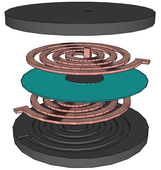
Figure 1: Split view of a monolithic tranformer. Ferrite is in black, coils in copper color and dielectric in green.
In the case of transformers or couplers, coils and dielectrics are assembled and put in a crucible on a ferrite powder bed and covered with ferrite powder. The crucible is electrical conductor and composed of a cylinder closed by two pistons. The wall is pressed and electrical current is pulsed-in to heat very rapidly. This process is called Pulse Electrical Current Sintering (PECS), aka Spark Plasma Sintering (SPS), allows to sinter at lower temperature compared for other techniques and makes possible to sinter metal with oxides.
The ferrite powder has usually a specific composition. For compatibility with the technology and with the target frequency, Ni-Zn ferrite with copper substitution is used. Typical composition is (Ni1-xZnx)1-yCuyFe2O4 , where 0.1<y<0.2 and 0.2<x<0.6. The Zn content can be tuned on demand depending on the temperature of operation.
DEVELOPMENT STAGE
The main difficulty that had to be solved with this technology was the electrical insulation between the primary and secondary coils. Technical solutions have been found, so today fully functional transformers have been realized and tested. At the present stage and due to the limitation of the PECS machine at our disposal, the external diameter is 20 mm and the thickness is 4 mm. However the technology is perfectly scalable and industrial PECS machines can produce parts as large as 550 mm.
The transmission band of the unloaded transformers is 30 kHz-10MHz which opens the possibility to operate over 1M Hz.
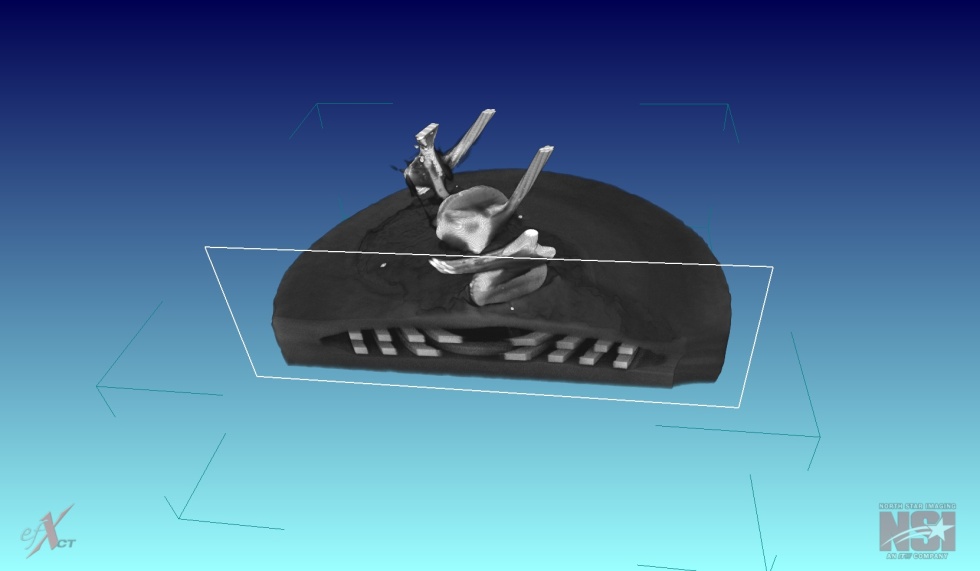
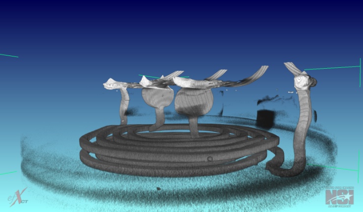
Figure 2: X-Ray tomography view of a transformer realized by the present technology. Right, global cut view; left, filtered view of coils
BENEFITS
The classical transformers made from today’s best commercial power ferrites can reach a power density of 20 W/cm3 at 1MHz. The first experiments with the present invention are already running at 40 W/cm3.
Because of the monolithic nature of the present invention, the thermal transfer from coil to core is strongly facilitated and because of the aspect ratio, thermo transfer from the core to the outside is also facilitated. In addition, these components can be either mounted on a heat sink. Under these conditions we expect to overtake the limit of 100 W/cm3.
Ultimately, such component could be mounted on the base plate of a power semi-conductor device, which is mounted on a heat sink.
INDUSTRIAL APPLICATIONS
This kind of components would be used in power electronics in any embedded application for which the power density is important from 10 W to at least several kW. They are particularly fitted for high frequency switch mode power supplies in electrical or hybrid vehicles, more electric aircraft or spatial technology.
For further information, please contact us (Ref 04951-01)