Describe : Additive and subtractive submicro-manufacturing
Référence
05975-01
Mots-clés
Statut des brevets
Priority patent application FR13 59713 filed on October 7th 2013 entitled “Procédé et système de structuration submicrométrique d’une surface de substrat”


N°FR2014052357 filed on September 23th 2014


Inventeurs
Thierry BELMONTE
Thomas GRIES
Rodrigo CARDOSSO
Cedric NOEL
Statut commercial
(non) Exclusive Licence or collaboration
Laboratoire
IJL Nancy
Description
CONTEXT
Additive manufacturing or 3D manufacturing developed quite rapidly last years from spreading from engineering teams and laboratories to production. These expression cover a large amount of different technologies allowing macroscale fabrication with polymers (now also reinforced by various particles) and some metals.
Microscale fabrication implies much more heavy and costly techniques requiring vacuum, ion beam as stéréo lithography or epitaxy which are additive techniques.
TECHNICAL DESCRIPTION
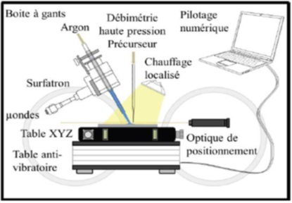
Our Describe technology allows microfabrication through addition or subtraction of material :
1. The precursor is injected through capillaries which diameter controls the precision of the spot/line.
2. The precursor is transformed in the neighbourhood of the substrate ‘surface thanks to the cold plasma and the material is formed on the surface. In case of reaction between the precursor and the substrate, the material can be peeled off.
Spots or lines (100nm width) may be superposed, formed with different materials at each step…The XYZ displacements of the table are driven by the computer depending on the design of the component to be realised.
DEVELOPPEMENT
The laboratory has developed the second generation of pilot scale equipment and first 3D pieces have been demonstrated (pyramids). Next step include alloy deposition, mixing of particles in the line during deposition; multilayers components…
CARACTERISTIQUES
1. width 100 nm
2. thickness 100nm to 2 μm in one step (one Z movement)
3. any material (even polymers) on any substrate (no temperature difficulty)
4. controlled atmosphere (N2) for some precursor (reaction of silane withy O2 for example) but always atmospheric pressure
5. speed of “writting” 10µm /min
6. material addition or ablation
APPLICATIONS
– MEMS
– Micro systems for health, optronics, photolithography masks,
– OLED
– Watch inductry
– Microprocessors
– Microfluidics
The Jean Lamour Institute created a technology which finds its way either in prototyping or fabrication of (micro)devices.
For further information, please contact us (Ref 05975-01)